- 您现在的位置:买卖IC网 > Sheet目录322 > DS28DG02E-3C+T (Maxim Integrated)IC EEPROM 2KBIT 2MHZ 28TSSOP
�� �
�
�DS28DG02:� 2Kb� SPI� EEPROM� with� PIO,� RTC,� Reset,� Battery� Monitor,� and� Watchdog�
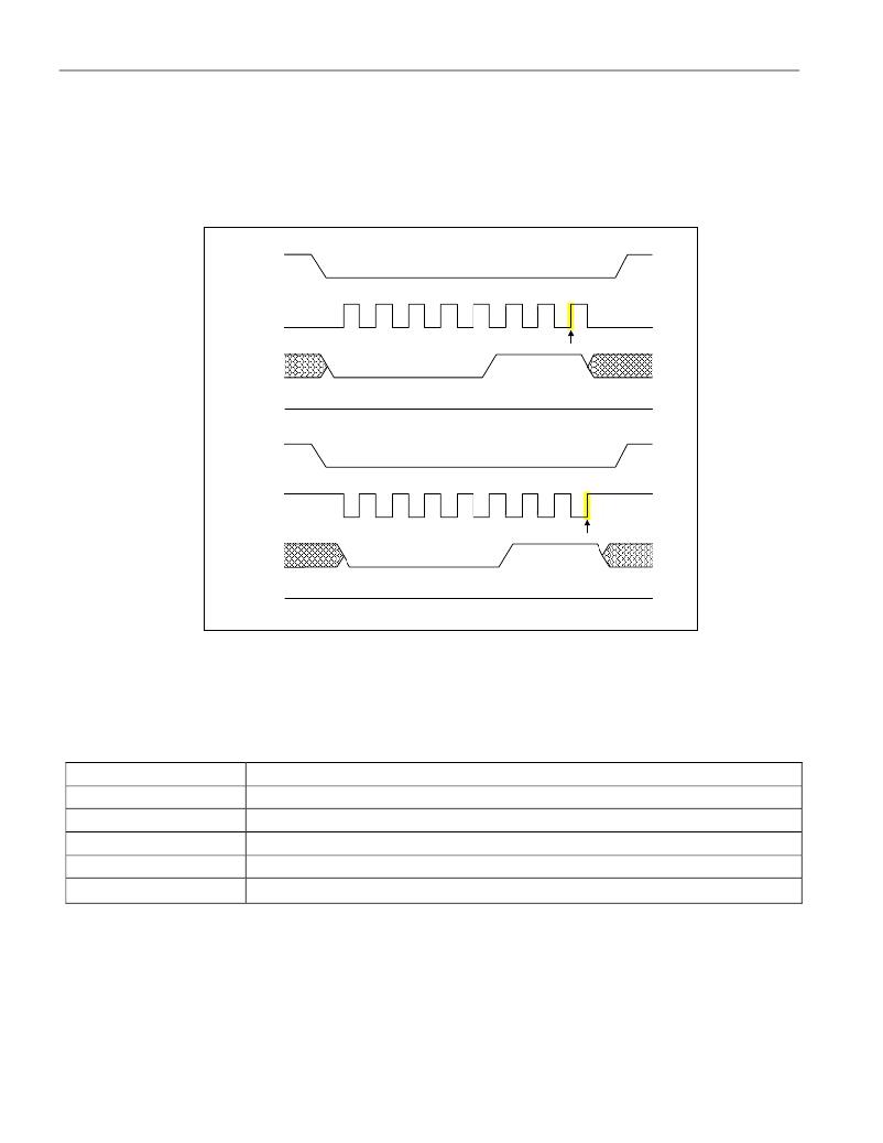
�RFSH� Refresh� PIO� Registers�
�The� volatile� PIO-related� registers� from� address� 120h� to� 125h� are� preset� with� their� power-on� default� values� stored� in�
�EEPROM� when� the� device� powers� up.� The� fastest� way� for� the� master� to� restore� the� power-on� state� without� power-�
�cycling� the� DS28DG02� is� through� the� RFSH� instruction.� The� RFSH� timing� diagram� for� both� SPI� communication�
�modes� is� shown� in� Figure� 17.� The� PIO� register� restore� begins� when� the� last� bit� of� the� instruction� code� is� clocked�
�into� the� device� (highlighted� SCK� transition)� and� ends� after� the� power-up� wait� time� (t� POIP� )� is� over.�
�Figure� 17.� Refresh� PIO� Registers� Timing�
�CSZ�
�Refresh,� Mode� (0,0)�
�0�
�1�
�2�
�3�
�4�
�5�
�6�
�7�
�SCK�
�SI�
�0�
�0�
�0�
�0�
�0�
�1�
�1�
�1�
�SO�
�CSZ�
�High� Impedance�
�Refresh,� Mode� (1,1)�
�0�
�1�
�2�
�3�
�4�
�5�
�6�
�7�
�SCK�
�SI�
�0�
�0�
�0�
�0�
�0�
�1�
�1�
�1�
�SO�
�High� Impedance�
�WRITE� Write� to� Memory� and� PIO�
�From� the� perspective� of� the� master,� the� DS28DG02� is� a� memory� device� with� memory� ranges� made� of� EEPROM,�
�SRAM� and� ROM.� Depending� on� the� memory� type,� the� behavior� of� the� device� upon� receiving� a� write� instruction�
�varies.� Table� 3� shows� the� cases� that� need� to� be� distinguished.�
�Table� 3.� Write� Access� Cases�
�STARTING� ADDRESS�
�000h� to� 0FFh�
�100h� to� 10Fh�
�110h� to� 11Fh�
�120h� to� 135h�
�136h� to� 1FFh�
�DESCRIPTION�
�User� memory� (can� be� write-protected� through� BP1:BP0).�
�EEPROM� registers� (reserved� and� power-on� default� values,� no� write-protection).�
�Read-only� memory.�
�SRAM,� PIO,� and� NV� SRAM� (may� be� write-protected� through� RPROT).�
�Nonexisting� memory.�
�The� four� blocks� of� user� memory� consist� of� 16� segments� of� 16� bytes� each.� The� first� segment� begins� at� address�
�000h� and� ends� at� address� 00Fh;� segment� 2� ranges� from� 010h� to� 01Fh,� etc.� Upon� receiving� a� write� instruction� with�
�an� address� targeting� the� user� memory,� any� data� bytes� that� follow� the� address� are� written� to� a� 16-byte� buffer,�
�beginning� at� an� offset� that� is� determined� by� the� 4� least� significant� bits� of� the� target� address.� This� buffer� is� initialized�
�(pre-loaded)� with� data� from� the� addressed� 16-byte� EEPROM� segment.� Incoming� data� replaces� pre-loaded� data.�
�With� every� byte� received,� the� buffer's� write� pointer� is� incremented.� This� allows� updating� from� 1� to� 16� bytes� starting�
�anywhere� within� the� segment.� If� the� write� pointer� has� reached� its� maximum� value� of� 1111b� and� additional� data� is�
�received,� the� pointer� wraps� around� (rolls� over)� and� the� incoming� data� is� written� to� the� beginning� of� the� EEPROM�
�write� buffer� and� continuing.� If� the� target� memory� is� not� write-protected� AND� the� WEN� bit� of� the� SPI� Status� register�
�24� of� 34�
�发布紧急采购,3分钟左右您将得到回复。
相关PDF资料
DS28E04S-100+T
IC EEPROM 4KBIT 16SOIC
DS28EC20+T
IC EEPROM 20KBIT TO92-3
DS301X
KWIK-CHG DESIGNATION STRIP SGL
DS3030W-100#
IC NVSRAM 256KBIT 100NS 256BGA
DS3045W-100#
IC NVSRAM 1MBIT 100NS 256BGA
DS3050W-100#
IC NVSRAM 4MBIT 100NS 256BGA
DS3065W-100#
IC NVSRAM 8MBIT 100NS 256BGA
DS3065WP-100IND+
IC SRAM 3.3V 8MB 34POWERCAP MOD
相关代理商/技术参数
DS28DG02EVKIT
功能描述:存储器 IC 开发工具 RoHS:否 制造商:STMicroelectronics 产品:Reference Boards 工具用于评估:M24LR64-R 存储容量:64 kbit 存储类型:EEPROM 工作电源电压:1.8 V to 5.5 V
DS28DG02G-3C+
功能描述:电可擦除可编程只读存储器 2Kb SPI 电可擦除可编程只读存储器 w/PIO RTC/Rst/Bat Mtr/Wtdg RoHS:否 制造商:Atmel 存储容量:2 Kbit 组织:256 B x 8 数据保留:100 yr 最大时钟频率:1000 KHz 最大工作电流:6 uA 工作电源电压:1.7 V to 5.5 V 最大工作温度:+ 85 C 安装风格:SMD/SMT 封装 / 箱体:SOIC-8
DS28DG02G-3C+T
功能描述:电可擦除可编程只读存储器 2Kb SPI 电可擦除可编程只读存储器 w/PIO RTC/Rst/Bat Mtr/Wtdg RoHS:否 制造商:Atmel 存储容量:2 Kbit 组织:256 B x 8 数据保留:100 yr 最大时钟频率:1000 KHz 最大工作电流:6 uA 工作电源电压:1.7 V to 5.5 V 最大工作温度:+ 85 C 安装风格:SMD/SMT 封装 / 箱体:SOIC-8
DS28E01-100
制造商:MAXIM 制造商全称:Maxim Integrated Products 功能描述:带SHA-1引擎保护的1K位1-Wire EEPROM
DS28E01-100_12
制造商:MAXIM 制造商全称:Maxim Integrated Products 功能描述:1Kb Protected 1-Wire EEPROM with SHA-1 Engine
DS28E01-100+
功能描述:电可擦除可编程只读存储器 RoHS:否 制造商:Atmel 存储容量:2 Kbit 组织:256 B x 8 数据保留:100 yr 最大时钟频率:1000 KHz 最大工作电流:6 uA 工作电源电压:1.7 V to 5.5 V 最大工作温度:+ 85 C 安装风格:SMD/SMT 封装 / 箱体:SOIC-8
DS28E01G-100+R
制造商:DALLAS 制造商全称:Dallas Semiconductor 功能描述:1K-Bit Protected 1-Wire EEPROM with SHA-1 Engine
DS28E01G-100+T
制造商:DALLAS 制造商全称:Dallas Semiconductor 功能描述:1K-Bit Protected 1-Wire EEPROM with SHA-1 Engine